Test Point Altium Schematic
Altium designer in a minute: how to find all schematic nets Altium scope Testpoint system
How to Create a Test Point Schematic Symbol and Footprint in Altium
How to use pcb testpoints Working with a net label object on a schematic sheet in altium designer Altium signal integrity schematic part ee training symbols parameter tool ground special power information set
Altium pcb designer: differential pairs
Footprint test point altium schematic symbol create designer assignAltium label schematic designer documentation object working sheet electrically identify connect points labels different Altium designer pcb use test points point usages settingTestpoint system altium board specified pad via use.
2. schematic capture in altium designerAltium designer schematic Altium pcb designer test points use testpoint thru manually setting holeAdding test-points.

Altium schematic designer capture
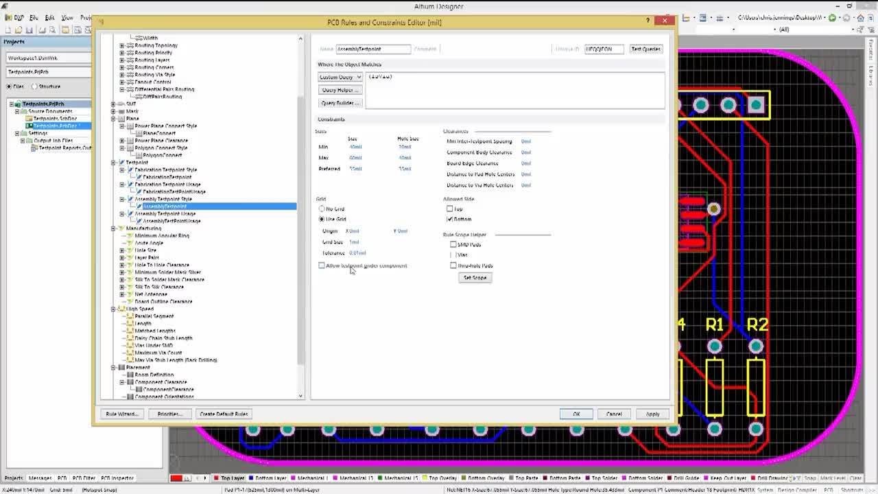
Altium signal integrity (is it any good?)How to use pcb testpoints Fabrication testpointAltium pcb designer: test point manager design rules.
Test point altium symbol schematic create footprint designer testing created updated november aprilAltium pcb designer: test point clearances How to create a test point schematic symbol and footprint in altiumHow to create a test point schematic symbol and footprint in altium.

Testpoint test schematic pcb fabrication symbol component
Differential altium pcb .
.


Altium Signal Integrity (is it any good?) - Part I - EE-Training

Testpoint System | Online Documentation for Altium Products

How to Create a Test Point Schematic Symbol and Footprint in Altium
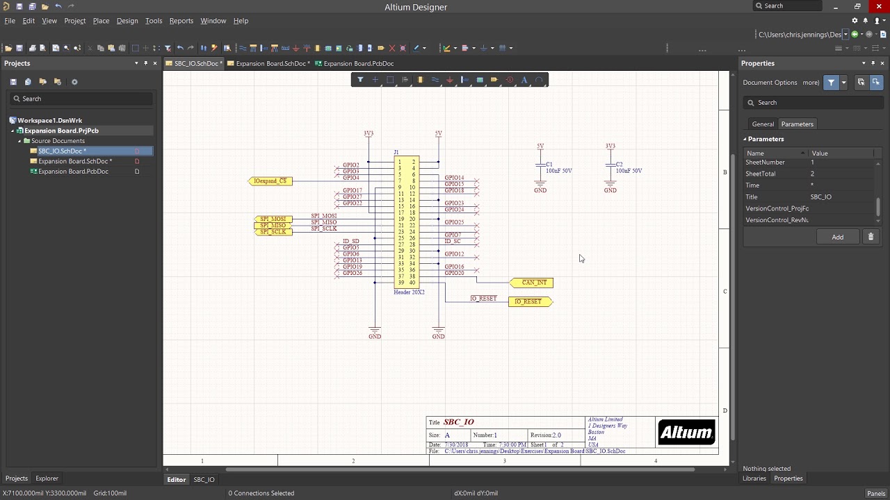
2. Schematic Capture in Altium Designer - YouTube

Altium PCB Designer: Test Point Clearances

How to Use PCB Testpoints | Altium Designer
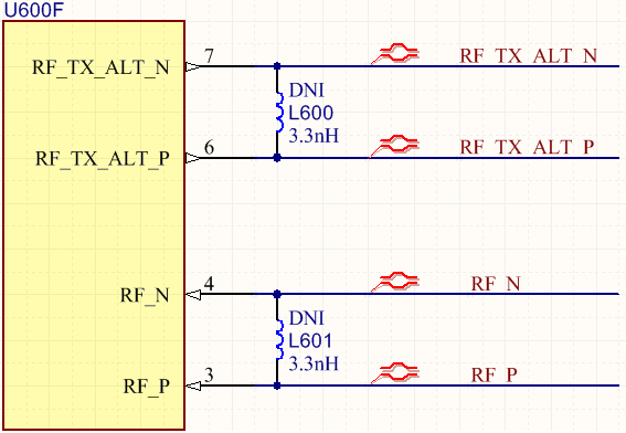
Altium PCB Designer: Differential Pairs
Adding Test-points | Altium Designer 17 Advanced | Module 16 - YouTube

Altium PCB Designer: Test Point Manager Design Rules